Simulating the STM profile of CO on Pd(110)
Purpose: Demonstrates the use of CASTEP for simulating the transmission microscope (STM) profile of a system.
Modules: Materials Visualizer, CASTEP
Time: 
Prerequisites: Adsorption of CO onto a Pd(110) surface
Background
The scanning transmission microscope (STM) provides an image of a material, but it can also be used to provide quantitative information at the atomic scale. The ability to simulate the STM image therefore provides a way to compare computed results with experiment.
CASTEP models the STM profile by representing it as an isosurface of the electron density generated only by states at a certain energy away from the Fermi level. The distance from the Fermi level corresponds to the applied bias in STM experiments: positive bias corresponds to empty (conduction) states and negative bias to occupied (valence) states. This approach neglects the actual geometry of the STM tip.
STM profile visualization makes sense only for models that represent surfaces in the slab supercell geometry. In addition, information about charge density at a distance from the surface is likely to be inaccurate as a result of DFT failing to reproduce the asymptotics of the wavefunction decay into a vacuum.
Introduction
In this tutorial, you will use CASTEP to simulate the STM profile of a CO molecule adsorbed onto a Pd(110) surface. The aim of the tutorial is to check whether STM is likely to confirm that the 2x1 structure found in the tutorial "Adsorption of CO onto a Pd(110) surface" is more stable or whether there will be little difference observed between the 1x1 and 2x1 systems. You will make use of results obtained previously for this system.
This tutorial covers:
- Getting started
- To run the calculation
- To create an STM isosurface
- To add extra information to the STM isosurface
In order to ensure that you can follow this tutorial exactly as intended, you should use the Settings Organizer dialog to ensure that all your project settings are set to their BIOVIA default values. See the Creating a project tutorial for instructions on how to restore default project settings.
Begin by opening the Materials Studio project that you created for the tutorial Adsorption of CO onto a Pd(110) surface. If you have not performed this tutorial or if you did not save the project files, you must do so before proceeding.
Select File | Open Project... from the menu bar to open the Open Project dialog. Navigate to the CO_on_Pd.stp project and click the Open button.
You will use the Pd(1 1 0) surface with CO adsorbed for this calculation.
Open the file (1x1) CO on Pd(110).xsd in the (1x1) CO on Pd(110)\(1x1) CO on Pd (110) CASTEP GeomOpt folder.
Click the CASTEP button  on
the Modules toolbar then select Calculation or choose Modules | CASTEP | Calculation
from the menu bar.
on
the Modules toolbar then select Calculation or choose Modules | CASTEP | Calculation
from the menu bar.
This opens the CASTEP Calculation dialog.
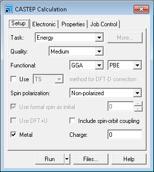
CASTEP Calculation dialog, Setup tab
Since you have already run a geometry optimization on the system, you only need to perform a single point energy calculation in order to obtain the orbitals.
Change the Task to Energy.
On the Properties tab check the Orbitals checkbox and ensure that you uncheck any
other properties.
On the Electronic tab click the More... button to open the CASTEP Electronic Options dialog. On the k-points tab ensure that the Custom grid parameters radio button is selected and that the Grid parameters fields are set as a to 3, b to 4 and c to 1.
Click the Run button.
The job is submitted and begins to run.
Repeat the same procedure for the optimized 2x1 structure in (2x1) CO on Pd(110).xsd located in the (2x1) CO on Pd(110) folder, making sure that the k-points Grid parameters are set as a to 2, b to 3 and c to 1.
Click the Run button on the CASTEP Calculation dialog and close both dialogs.
When the job has finished, you should save the project.
Select File | Save Project from the menu bar.
3. To create an STM isosurface
When the calculation finishes, you can display the charge density difference. Begin by closing all the open windows.
Select Window | Close All from the menu bar.
Now open the output structure for the (1x1) and (2x1) calculations side by side.
Open (1x1) CO on Pd (110).xsd in the (1x1) CO on Pd (110) CASTEP Energy folder.
Also open (2x1) CO on Pd(110).xsd in the (2x1) CO on Pd (110) CASTEP Energy folder. Select Window | Tile Vertically from the menu bar.
Make (1x1) CO on Pd (110).xsd the active document and open the Display Style dialog. On the
Lattice tab set the Max. value of the range in the A direction to 2.00, in the B direction to 2.00, and in the C direction to 0.90. Select the (2x1) CO on Pd(110).xsd document and change the Max. ranges to 2.00 in the B direction and 0.90 in the C direction.
To better differentiate between surface and adsorbate, you may want to change the Atom display style of all Pd atoms.
For each document, select one atom of each Pd layer. On the Atom tab of the Display Style dialog, select the CPK radio button and change the CPK scale to 0.9. Close the Display Style dialog.
Orient both structures such that the (110) surface rows are facing the same way.
The models should look similar to the images below.
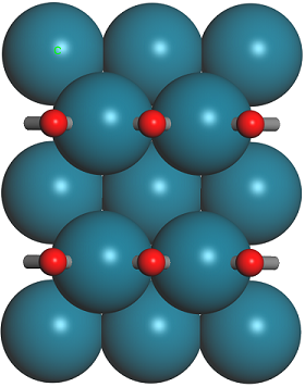
1 × 1 and 1 × 2 supercells of CO on Pd(110)
Take a note of the z-coordinate of the oxygen atoms in either case, they should be approximately 5.4 and 5.3 Å.
4. To add extra information to the STM isosurface
Now you will import the volumetric information into the two structure documents.
Click the CASTEP button on the
toolbar, then select Analysis from the dropdown list to open the CASTEP Analysis dialog. Select STM profile from
the list.
Open (1x1) CO on Pd (110).castep and ensure this is listed as the Results file. Set the value of STM bias to
1.0 and uncheck the View isosurface on import checkbox. Make (1x1) CO on Pd (110).xsd the active document and click the Import button.
Repeat this for the (2x1) CO on Pd (110).castep output document and the (2x1) CO on Pd (110).xsd structure. Close the CASTEP Analysis dialog.
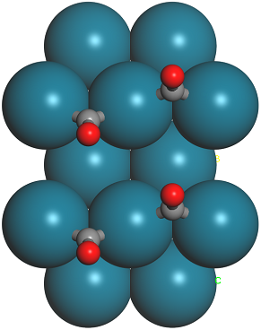
The next step will be to create simulated images to model STM experiments in the constant height mode for our two structures. This can be achieved by displaying slices through our simulated STM volumetric information.
On the Volume Visualization toolbar, click arrow for the Slice button  and select Parallel to A & B axis. Repeat for the other document.
This procedure creates a volume slice that will become our STM images. Scanning tunneling microscopy is usually done well above the actual atoms in any experiment and relies on tunneling. To mimic this setup in our simulation, we have to set our slice relatively high above the oxygen atoms, but also well away from the bottom periodic images of the Pd atoms. A value of 1.0 Å above the O atoms is a good compromise, as long as we remember to compare like with like and set the same value for both simulations.
For high-quality STM simulations in research problems, you will have to go at least 3 Å higher above the highest atom and use an accordingly large unit cell height. To achieve a reasonable resolution of your simulations, you may have to significantly increase the plane wave cut
We now have to adjust the color scale to show the relevant information.
Select the Slice and click the Color Maps button  . Use the right-arrow
  buttons to set the From and To values to the SliceMappedMin and SliceMappedMax values shown in the Properties Explorer respectively. Change the Spectrum to Black-White and set Bands to 128.
Repeat this for the other document and close the Color Maps dialog.
In complex simulations, an estimate of the relative brightness for different adsorbates may be obtained if the color scales are identical. However, this only works if all the settings in all calculations are absolutely identical.
You may want to change the representation such that a part of the periodic surface is not covered by the slices. Your final results should look similar to this:
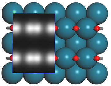
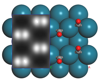
1 × 1 and 1 × 2 Supercells of CO on Pd(110) with simulated STM profile. The calculated volume slice on the left side of each image corresponds to the predicted STM contrast, while the extended supercell shows the location of the atoms underneath the STM image.
According to this simulation, it should be very easy to distinguish between the 1 × 1 and 2 × 1 structures of CO adsorbed on Pd(110) in an STM simulation. The shape of the STM image suggests that the contrast is mainly due to the π-orbitals of the CO molecule. which are aligned in the 1 × 1 supercell, but offset in the 2 × 1 structure. The volume slice is constructed from the density due only to orbitals corresponding to the bias, that is, those about 1 eV above the Fermi level. The color corresponds to the total density of states, with the white regions corresponding to the highest DOS.
This is the end of the tutorial.